In the next article we are going to take a look at gEDA. This is a software environment for the automation of electronic designs that users will be able to use in the design of electrical diagrams, printed circuits and simulations.
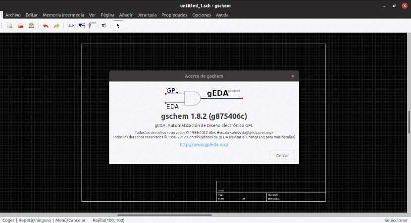
The gEDA project has produced and continues to develop a full open source suite and electronic design automation toolkit. The name of the project comes from the GPL for the license, and from the acronym in English Electronic Design Automation tools (electronic design automation tools). The license is under the terms of the GNU GPL, which lists it as free software.
The gEDA project was started due to the lack of free EDA tools for POSIX systems. The suite is being developed mainly on the GNU / Linux platform. In addition, a certain effort is being made by the developers to ensure that the tools run on other platforms as well.
These types of tools are used for electrical circuit design, schematic capture, simulations, prototyping, and production. Currently, the project gEDA offers a set of free software applications for electronic design. These include tools for schematic capture, attribute management, bill of materials generation (GOOD), network lists in more than 20 network list formats, for analog / digital simulation and for printed circuit boards (PCB). gEDA is mainly oriented towards the design of printed circuit boards, unlike integrated circuit design.
General characteristics
The gEDA suite is a set of programs. Some of those they include are the following:
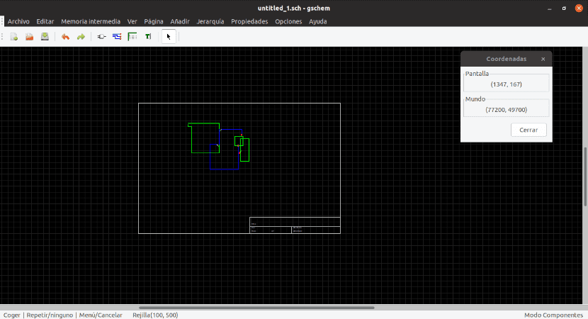
- We can draw electronic schematics, which describe the logical structure of a circuit with the gschem tool. Schematics are made up of symbols, which represent the various components of the circuit, and are obtained from a standard library or from those created by the user. Connections between components are represented by networks (cables).
- We will have available gattrib, Which is a spreadsheet-like program for bulk editing of component attributes.
- We will have a library of functions such as libgeda to manipulate the gEDA schema and symbols.
- With netlist we will have a highly flexible and hierarchy-sensitive utility that analyzes the schemas to generate a series of results. These include network lists for a wide variety of network design tools. PCB. We can also generate bills of materials and reports of DRC for our schemes.
- We will be able to use a command line utility such as gsch2pcb to streamline workflow where it is used 'PCB' Y 'gschem'.
- gsymcheck is a utility to check common errors in schematic symbol files.
- The command line utility Gave implements the settings of the above programs, the export of schematics and symbols to various formats in addition to the shell for command-line processing of our data.
Installing gEDA on Ubuntu
If you want to have this software in Ubuntu, it can be installed in several ways. The first will be by opening a terminal (Ctrl + Alt + T) and writing the following script in it:

sudo apt update && sudo apt install geda pcb gerbv
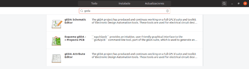
If you prefer not to use the terminal, you can also install this program from Ubuntu software option. You just have to open it and look for "in gear".
After installation, whatever option you use, the software can be launched by searching for the corresponding launcher on our computer.

It can get more information about this project in your web page. Information can also be found in your Wiki or the documentation section that we will find within the Wiki. Any questions about this project, I think it can be resolved in the FAQ section.
If you would like to consult designs created with gEDA, you can do it through the project gallery which can be found on your Wiki.